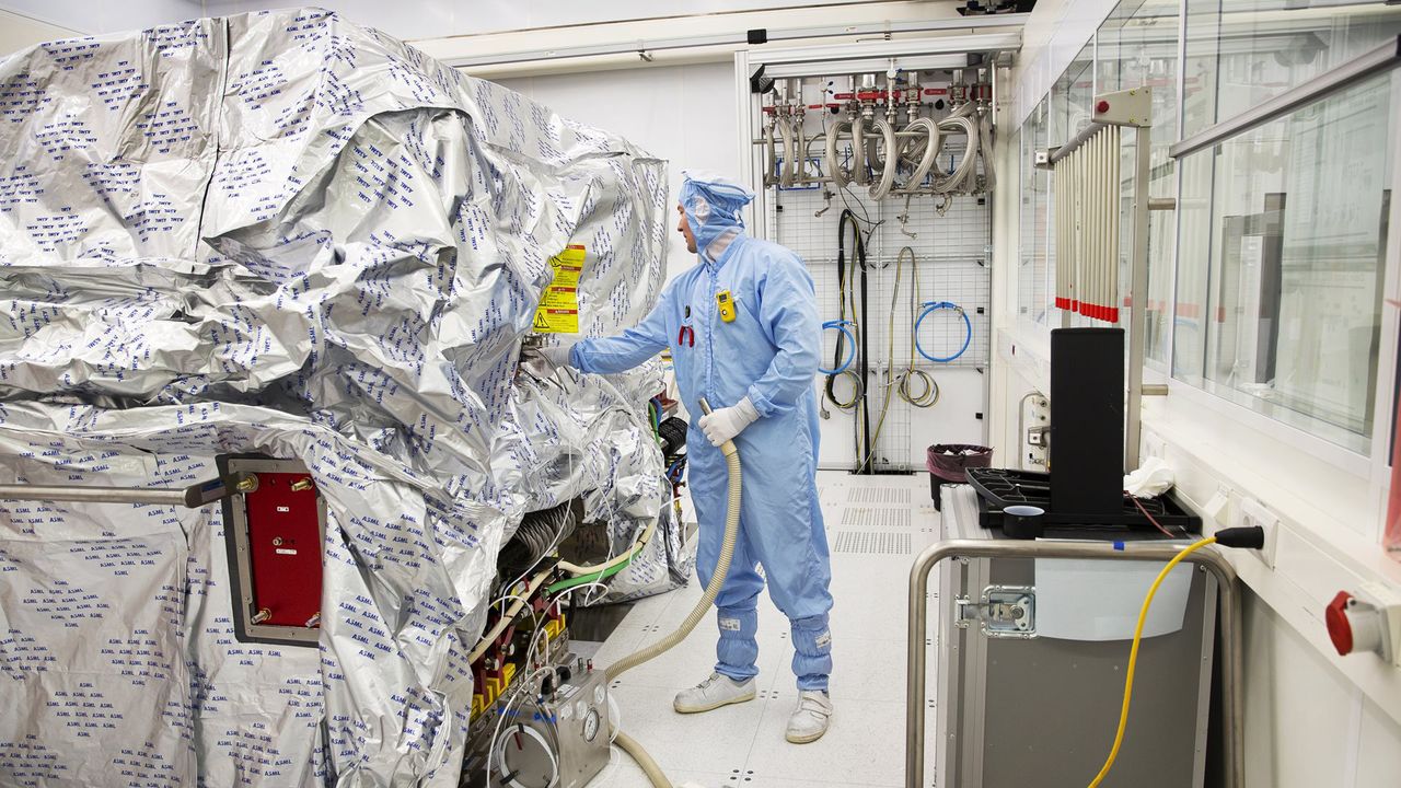
Intel is leading the semiconductor industry with High-NA fleet and process-maturity milestone as it reaches 1 million wafers processed using High-NA tools, moves forward with 6×12 photomask effort.
Intel surpasses one million High-NA EUV wafers processed, outpaces the rest of the industry combined — company also trailblazing giant 6×12 photomasks to speed production and lower costs
Intel surpasses one million High-NA EUV wafers processed, outpaces the rest of the industry combined — company also trailblazing giant 6×12 photomasks to speed production and lower costs
- 何が変わったか
- Intel is leading the semiconductor industry with High-NA fleet and process-maturity milestone as it reaches 1 million wafers processed using High-NA tools, moves for
- 誰に関係するか
- AI導入担当者・事業責任者 ※タイトル・要約からの推定
- 次に確認すること
- 自社の利用環境・契約への影響を確認 ※タイトル・要約からの推定
このニュースの背景・続報
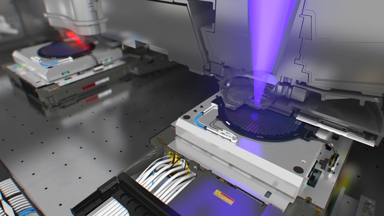
編集メモ: IntelのHigh-NA EUV技術における圧倒的な生産実績と大判フォトマスクの導入は、半導体微細化の限界突破を意味し、次世代プロセッサの性能向上とコスト削減を通じた業界地図の変化を予見させます。
自動判定による詳細な影響を見る
EDITORIAL SIGNAL
重要度 中このニュースの影響
製品選定や業務・開発手順に影響する可能性があります。
影響を受ける人
- AI導入担当者・事業責任者
- 調達・経理・サービス運用担当者
確認すること
- 自社の利用環境・契約への影響を確認
- 現契約と利用量から費用変化を試算
今後の注目点
公式発表、提供条件、利用者への実際の影響
タイトル・要約の語句に基づく自動判定です。最終判断は公式発表・一次資料をご確認ください。